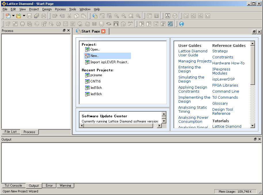
Lattice Diamond memo
Suns & Moon Laboratory
2011-09-04
Verilogメモ
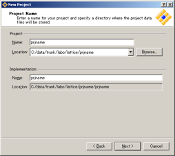
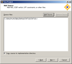
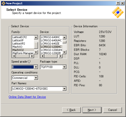
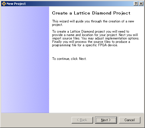
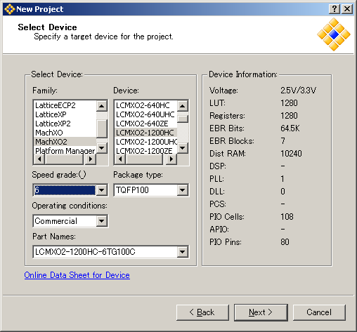
プロジェクト生成
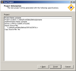
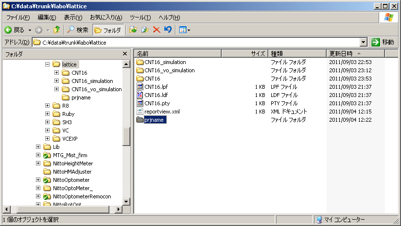
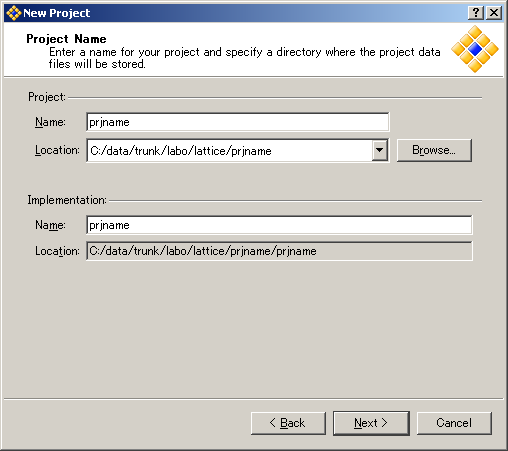
先にプロジェクトフォルダ(Project Name)を掘っておく
Project Locationを先ほど掘ったフォルダにする
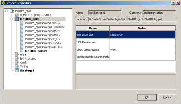
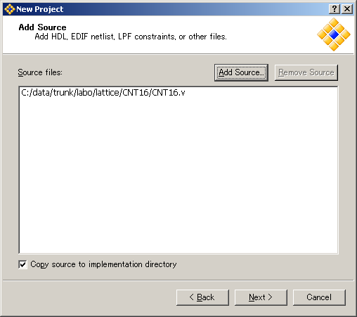
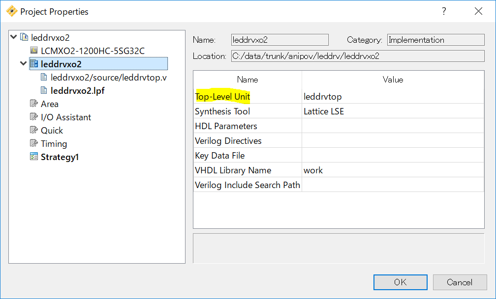
最後にトップレベルモジュールを指定。(Project->Property Pagesで、)


トップレベルモジュール設定
Project -> Active Implementation -> Set Top-Level Unit
 ver3.10.2.115
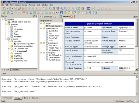
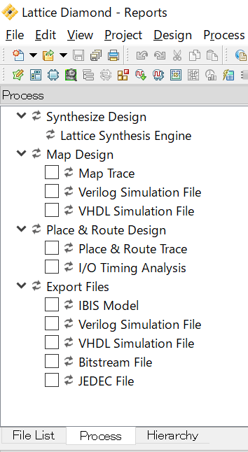
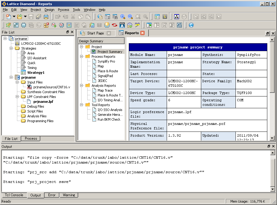
Process
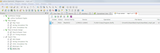
Process ViewはRun(ビルド)したりするタブ
ピンアサイン
GUIでピンアサイン
1回コンパイル
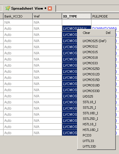
Spreadsheet Viewの下にあるPin Assignmentsタブで割り付け。(全ピン表示)
Spreadsheet Viewの下にあるPort Assignmentsタブで割り付け。(使用ポートのみ表示)
Pin Layout Fileでピンアサイン
一回コンパイル。コンパイルしないとインポート出来ない
File->Import->Pin Layout File
File->Save All
再度コンパイル
Verilogでピン属性
コメント内のsynthesisでいろいろ指定可能
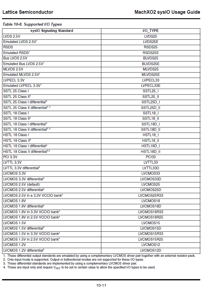
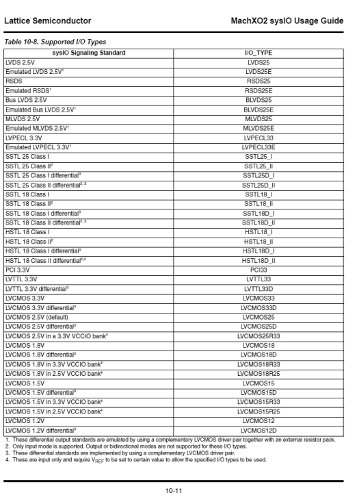
TN1202 MachXO2 SsysIO Usage Guide P19
/* synthesis name=value */
ピン配置例
	output	[11:0]	CK; /* synthesis loc="11,12,13,14,16,17,20,21,23,25,27,28" */ // to HD107S CLK
	output		DT; /* synthesis loc="5" */
I/O_TYPEは指定しても効果が無い(Diamond3.11.2.446)
I/O_TYPE
まとめて選択して右クリックで指定が簡単。
synthesisでのI/O_TYPE指定は効果が無い(Diamond3.11.2.446)
シミュレーション
Tools->Simulation Wizard
で、SDF付きのシミュレーション設定ファイルが作成出来る。
けれど、なぜかライブラリ設定がされていない。
Active-HDL起動したら、自分でライブラリ設定する。
Active-HDL
内蔵オシレータ
こんな感じでOSCHを定義する。指定できる周波数は決まっているので、表を見て決定する。
// TN1199J_rev2.5_MachXO2sysCLOCKPLLDesignandUsageGuideJapaneseLanguageVersion.pdf
// Page 13-29 Table13-15.supported frequency
// Page 13-30 Verilog
defparam OSCH_inst.NOM_FREQ = "24.18";

OSCH OSCH_inst(
	.STDBY(1'b0), // 0=Enabled, 1=Disabled  also Disabled with Bandgap=OFF
	.OSC(clk),
	.SEDSTDBY()  // this signal is not required if not using SED
);
IP Express
Tools -> IP Expressで起動
ツリーからモジュール選択して、ファイル名設定してCustomizeボタン押す。
ダイアログ表示されるので、パラメータ設定して、Generateボタンを押す。
IPXファイル
verilog使う場合は不要っぽい
第五章モジュール/IPO生成 2015年6月 5-1
module_IP_gen_rev3.3__1.pdf
.ipxファイルはツールが必要なパラメータ情報を全て含む、Diamond固有のテキストファイルです(ユー
ザは編集しないこと)。ipxファイルを取りこむ利点は、パラメータの変更が容易な点があります。プロジェ
クト進捗に伴い、或いはその他要因で変更する可能性がある場合は、.v/.vhdではなく、.ipxが良いでしょ
う。.ipxの当該行をダブルクリックすると、指定済みのパラメータをロードした状態で再び図5-7のような
パラメータ設定GUIが表示されます。他方、インスタンスする場合やソース記述をチェックしたい場合は
.ipxは不都合ですので.vや.vhdを参照する必要があります(勿論、論理シミュレーションに.ipxを用いるこ
とはできません)。
Error VCP6251
ActiveHDL9.1
以前作ったWorkSpaceコンパイルしたらエラー
# Error: VCP6251 Error in SLP repository: Incorrect SLP repository library version. Library: work must be recompiled. Use adel to clear your library and compile your sources again.
work libraryをDeleteしてからCompileAllしたら通った
書込み
ケーブルはVCC接続必要
ver2.0書込み
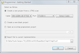
Diamond Programmerを使う。
Diamond統合だと書込み出来なかった。
ver1.3書込み
ispVM Systemを使う
設定ファイルはxcf
GOで書込み
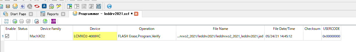
ver3.10書き込み
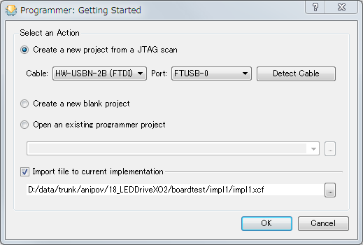
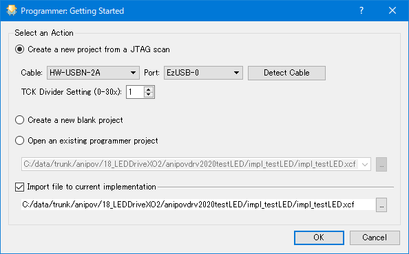
Tools->Programmer(黄色い下矢印アイコンクリック)
Programmerの緑下矢印アイコンクリックで書き込み
Deviceのデバイス名が黄色い時は、デバイスを確認出来なかった時みたい。その時は黄色いデバイス名クリックすると、デバイス名確定して書込可能になる。
ver3.11書き込み
★★★★ケーブルはVCC接続必要★★★★
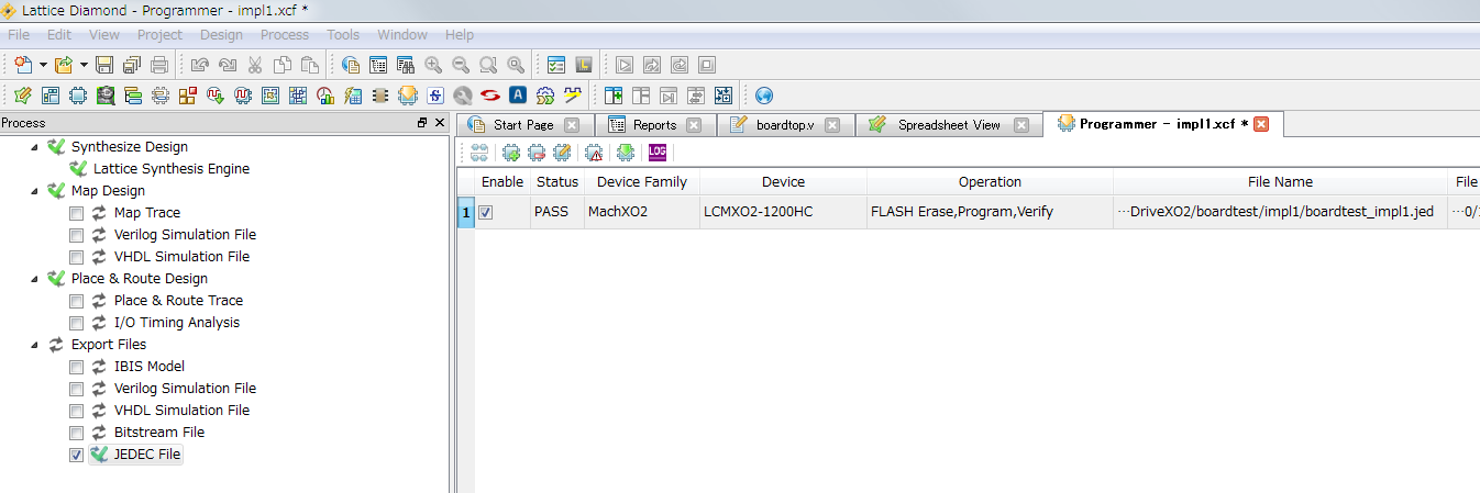
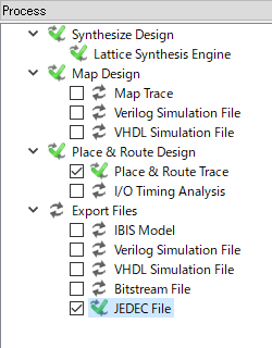
書き込みはJEDECファイルなので、JEDEC Fileを生成する。
★★★★Deviceのデバイス名が黄色い時★★★★
Deviceのデバイス名が黄色い時は、デバイスを確認出来なかった時みたい。その時は黄色いデバイス名クリックすると、デバイス名確定して書込可能になる。
接続した初回はなるっぽい。

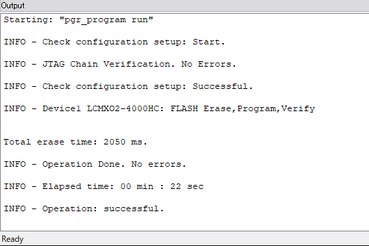
書き込みアイコンを押して書き込み

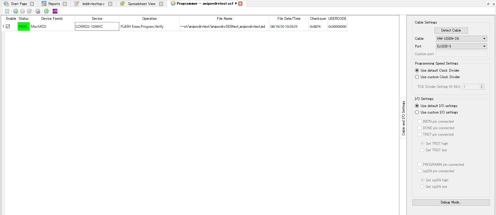
書き込み終了
vo出力
Process -> Export Files -> Verilog Simulation File
をやると、*.voを出力する。
MCLKの設定
Diamond3.10.2.115
Tools -> Spreadsheet View -> Global Preferencesタブ
sysConfig -> MCCLK_FREQで設定する
CLK範囲は、データシートTN1204参照
FAQ
未使用ピン
デフォルトはpull-up
(1033) Do the unused I/O pins need to be grounded in a device?
レジスタ初期値
0に初期化
(204) What is the initial logic level of a register after power-up?
GSRをRTLで使用していなければ、コンフィグ後リセットしてくれる。
(353) What is the state of FPGA Flip Flop outputs at power-up? The reset pins of my design ...
What is the state of FPGA Flip Flop outputs at power-up? The reset pins of my design registers are tied to neither GSR nor LSR.
Even if GSR/LSR are not used in RTL, GSR is always used during bitstream download to reset flip flops up to the point when download is complete.
So the state of a register's Q output is 0 at powerup. This assumes that clock input to the register is at steady state logic low.
未コンフィグのピン初期値
pull down(GND)
(1528) What is the default configuration of the I/O pins in a blank MachXO2 device ?
What is the default configuration of the I/O pins in a blank MachXO2 device ?
The default configuration of the I/Os in a blank MachXO2 device is tri-state with a weak pull-down to ground (GND).

Please follow the link in the MachXO2 Data Sheet - DS1035 under section "Architecture", on page 2-23, you can find further details about the behavior of a typical I/O during power-up.
富士エレクトロニクスの回答
2.同じくコンフィグ終了後のピンの状態について
(回答)
XO2の場合は、ブランク時もCFM書き込み後も、コンフィグレーション後
デフォルトも全て弱いプルダウンが有効になったトライステートです。
インストール
Diamond2.0からWindows7の64bit版がリリースされている。
1.x系は、1.4.2が最終
リモートデスクトップで動かない
リモートデスクトップでは動作しないようです。(ver1.3)
ライセンスの更新
サポートセンター→Licensingから、「Request Diamond Free License」
https://www.latticesemi.com/ja-JP/Support/Licensing
▼
Latticeにログイン
▼
NICのMACアドレスを調べて入力
▼
ライセンス要求ボタンを押す
▼
すぐにライセンスがメールで送られてくる(メールの遅延はあるが)
▼
古いLicense.datをメールで送られてきたLicence.datに置き換え
▼
次に起動するときは、新しいライセンスを読みこんで起動してくれる
2025-12-04 11:53:02 32400


 ver3.10.2.115